Power Packaging
The University of Arkansas High-Density Electronics Center has been engaged in power device and power electronic module research and development efforts for more than 10 years. HiDEC has complete processing, packaging, and assembly facilities for developing state-of-the-art power device and power electronic module packages. These facilities are also available for use by industry partners.
HiDEC Power Packaging Process
- Overview
- Power substrate
- High Temperature attach
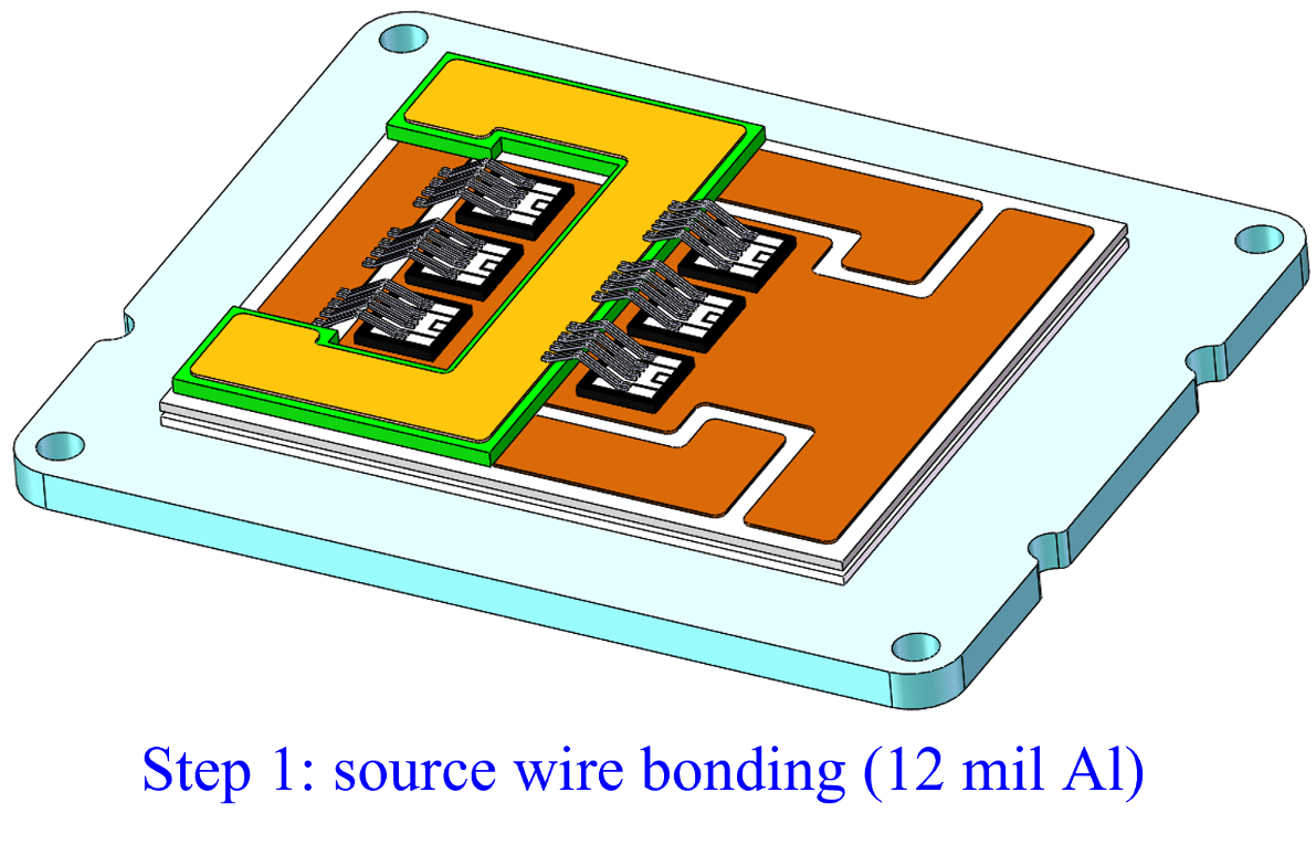
- Power wire bonding
- Gate/Kelvin board attach & Gate/Kelvin wire bonding
- Encapsulation
- Terminal bending
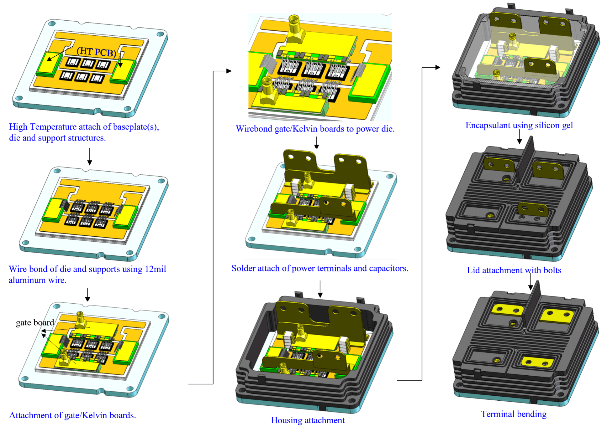
Power packaging consists of the creation of a packaging to integrate high-powered die in a module that can successfully operate at high voltage, high currents and high temperature. The graphic depicts the process flow for creating a module from the high temperature die attach through the encapsulation and lead bending of the power terminals. The design of the package is done in such a way to minimize both overall size and parasitic impedances. It is our goal to offer these package solutions for modules that can operate at 1.7kV, 3.3kV and 10kV. Our ability to fabricate low volume prototypes will enable reliability studies and downstream research projects to customers who do not possess these low-volume fabrication capabilities.
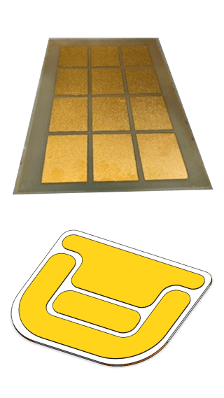 The power substrate base consists of a ceramic core sandwiched between two copper layers. The ceramic is typically aluminum oxide or aluminum nitride. There are two types of substrates available for module building; direct bond copper and active metal braze. These substrates are patterned from what is called a master coupon that is typically 125mm by 178mm in dimension. You will also see a need to create a double-stack of substrates to ensure proper voltage isolation between active components and the baseplate as the modules are designed for higher voltage operation (typically greater than >6.5kV).
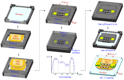
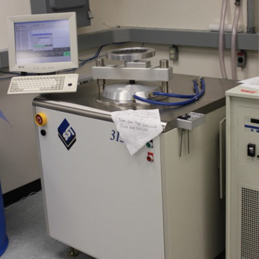
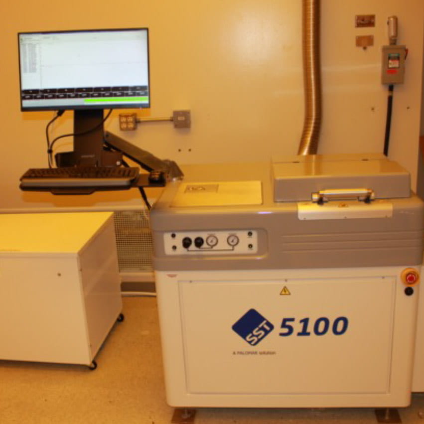
“In order to attach die to substrate(s) and substrate to baseplate in a precise position, the components are held in place by a custom-machined graphite fixture during the “high-side” reflow process. We distinguish high versus conventional, as the process will generally take two distinct solder processes. This first is done with solders that reflow at around 300⁰C. HiDEC has both a brazing and soldering tool for this purpose. The former (SST 3130HT) allows for temperatures beyond the standard 450⁰C while the latter (SST 5100) has a formic acid preclean option to remove metal oxides. Both systems use forming gas during the reflow process to again keep the surfaces clean thus allowing for the use of solder preforms without the use of flux.
 |
SST 3130HT brazing tooling |
SST 5100 solder reflow tooling |
|
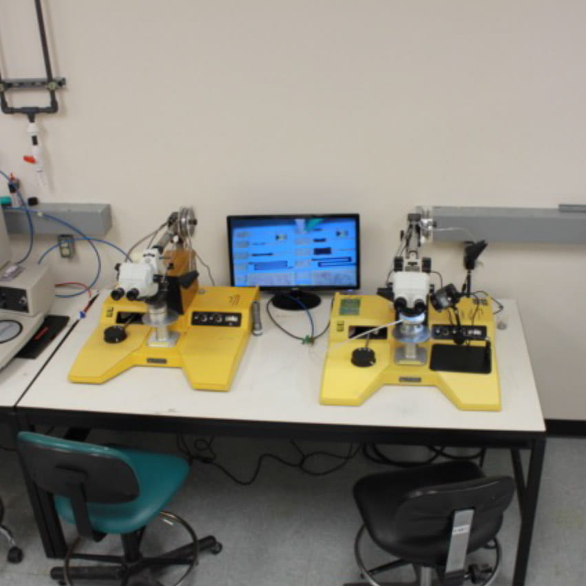
Orthodyne wire bonder |
Hesse wire bonder |
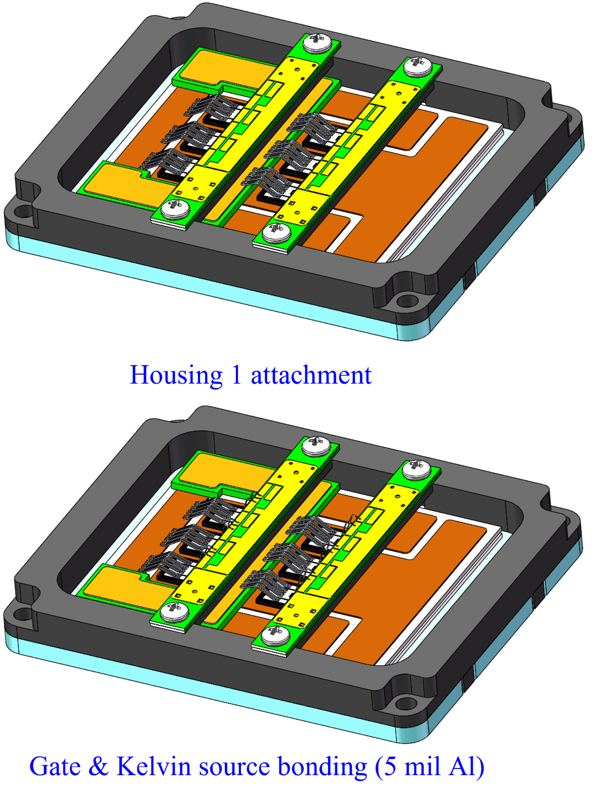
In order to attach the gate & Kelvin pads of the die to the control board electrically, wires are attached using a wire bonder. These control boards are usually integrated into the housing which is attached mechanically (screws) and chemically (glue) to the baseplate. Because of the size of the gate pad on the die, a smaller gauge wire (from 3 to 8mil in diameter) is placed on each die. HiDEC has a manual bonder for this service.
 |
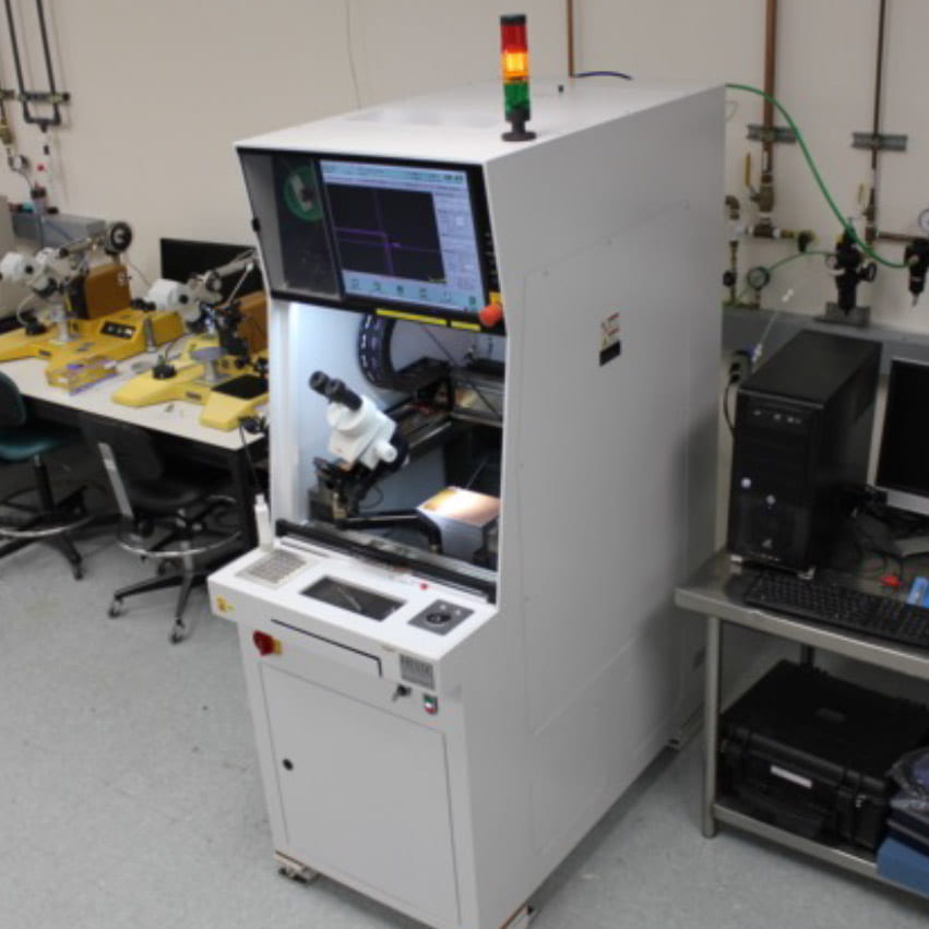
Orthodyne wire bonder |
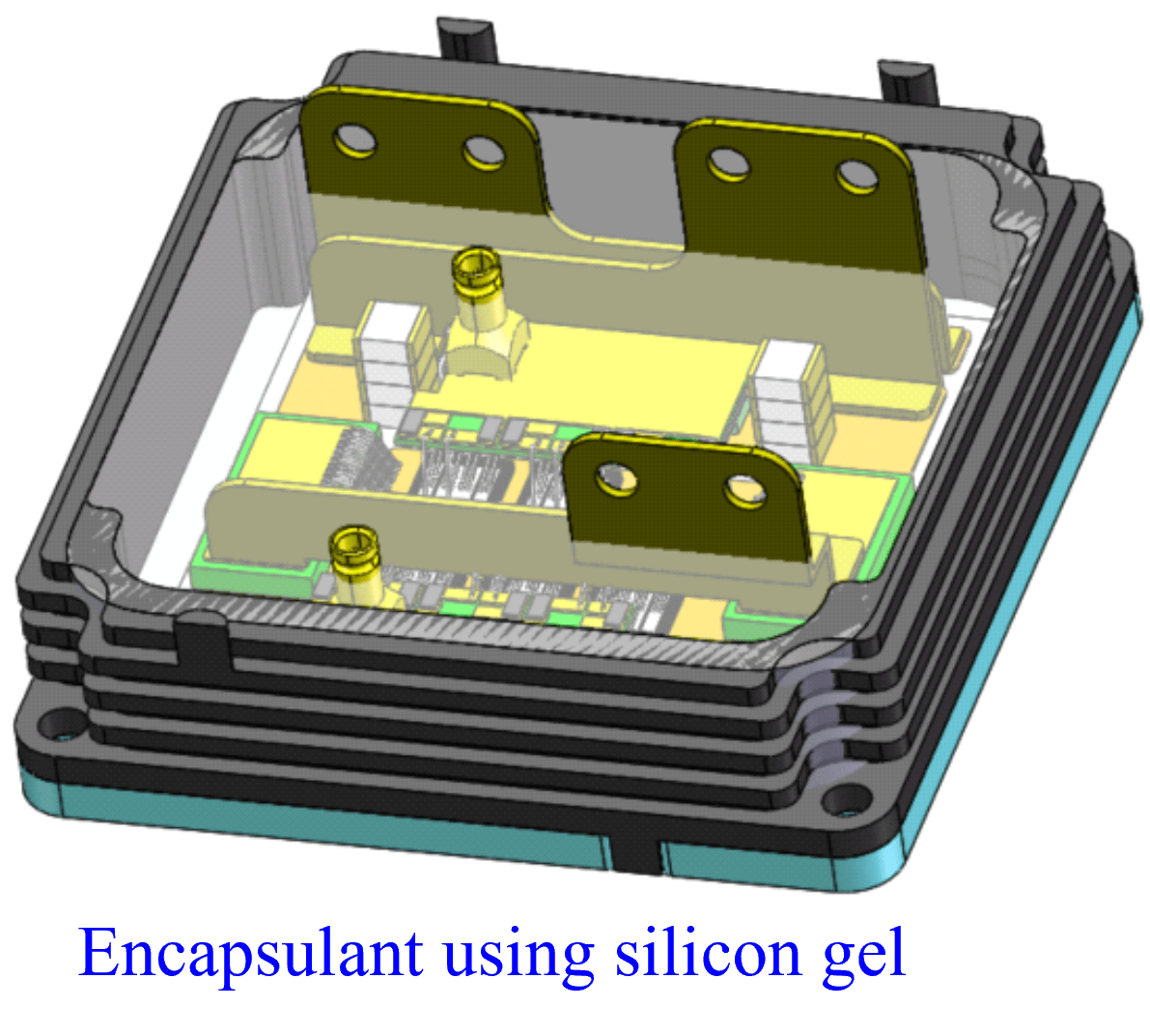
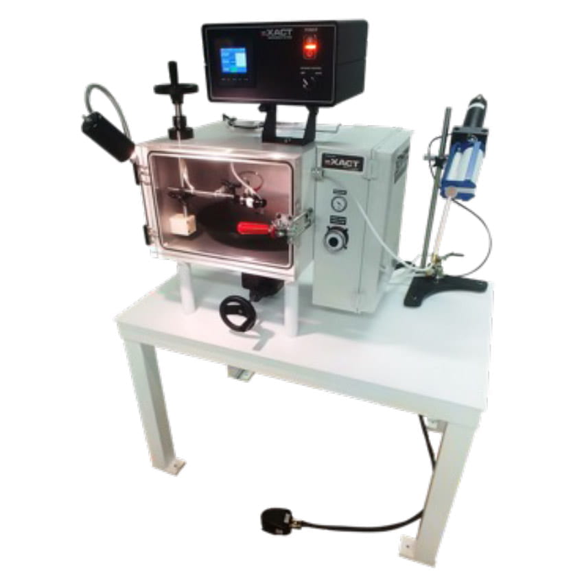
In order to ensure proper voltage isolation of the components inside the housing, a silicon get is dispensed inside. As it is important that no voids of air appear in this process, the dispensing is done while the module is under vacuum. The Exact Dispensing VC-18 Vacuum Chamber System is used for this purpose.
 |
Encapsulant tool |
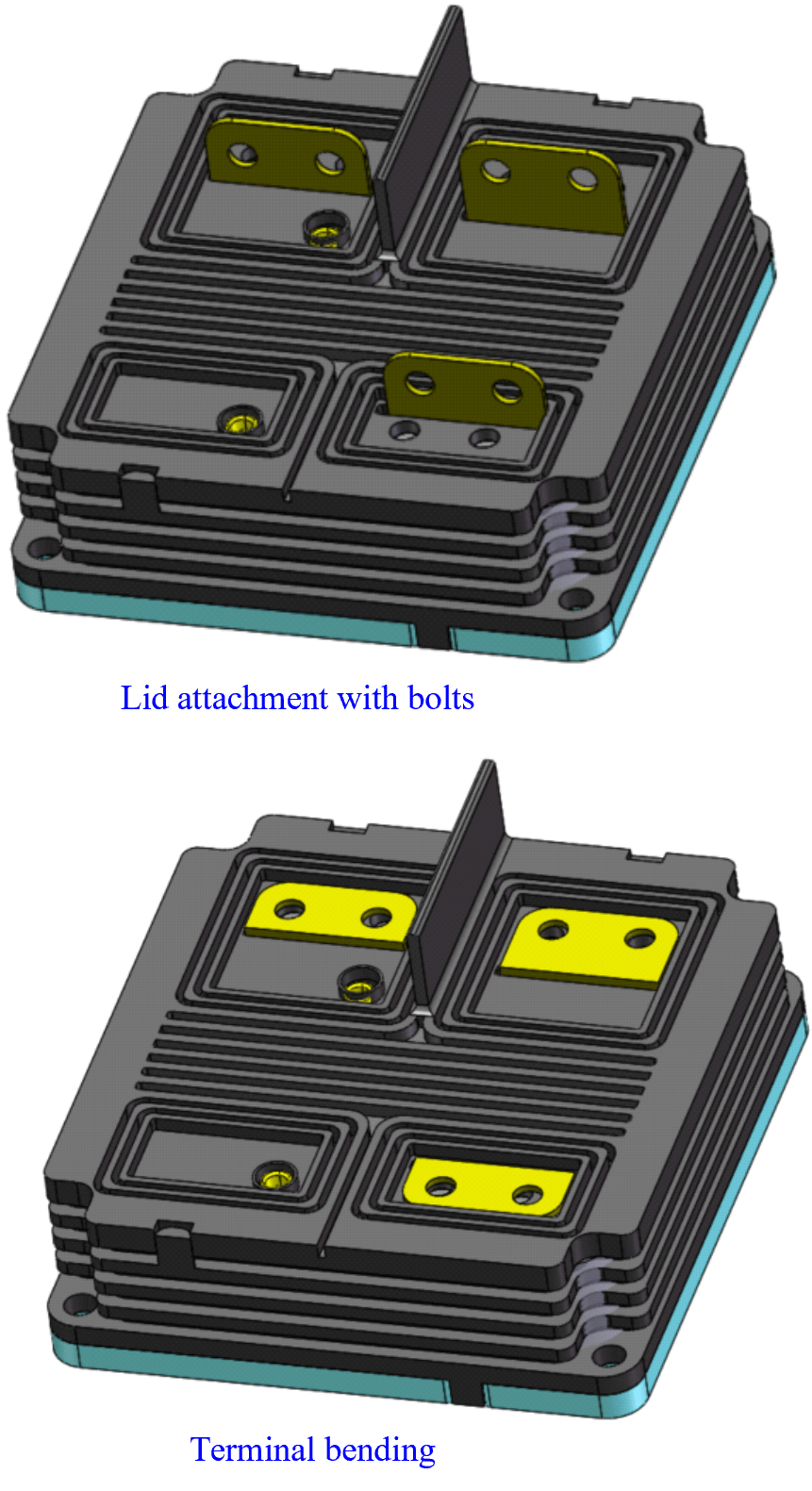 With the encapsulation in place, the lid is attached, and the leads bent in place to allow for functional and reliability testing.