Research
Our work over the years is briefly described below.
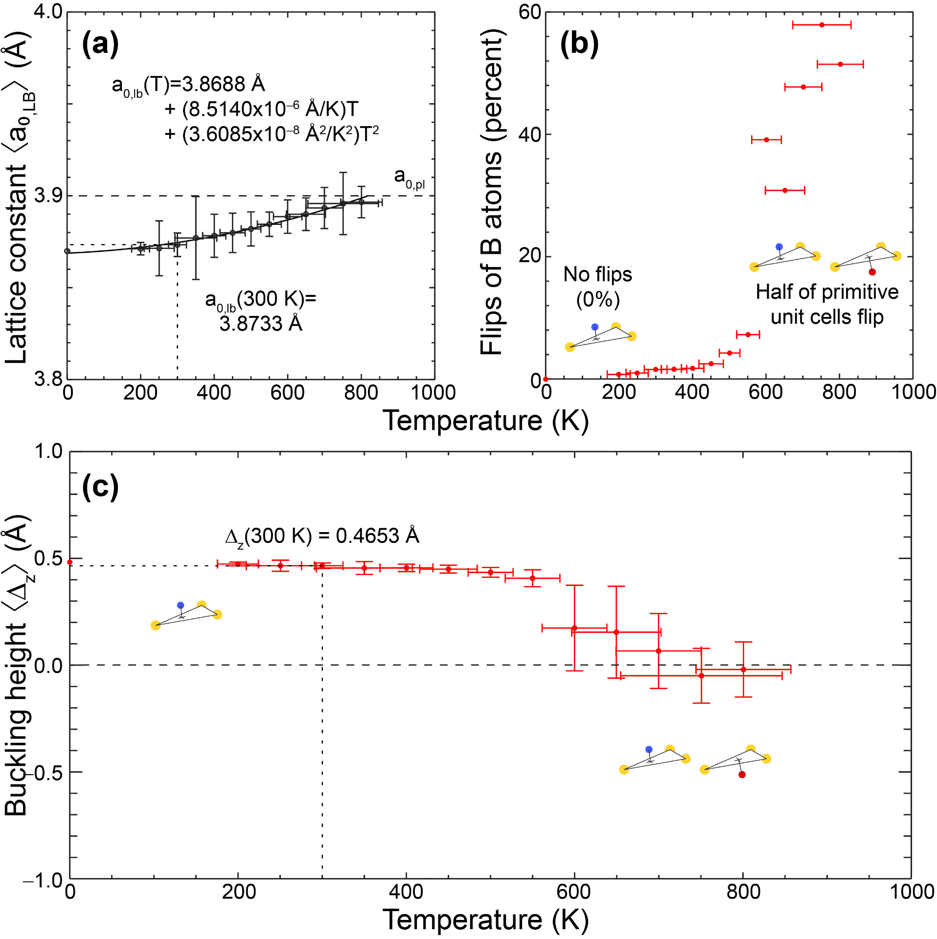
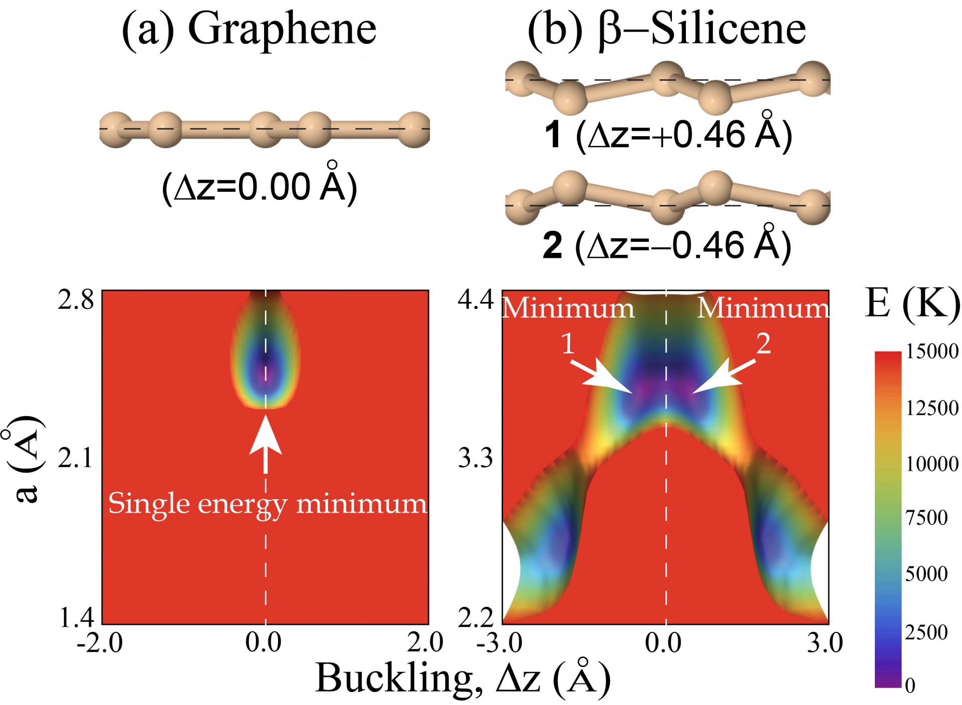
Uncovering a paraelastic phase in freestanding silicene at finite temperature
The low-buckled silicene has a ferroelastic (double-degenerate) ground state, and we observe a structural transition onto a planar structure on average. See Publication 67.
Creating a three-dimensional intrinsic electric dipole on rotated CrI3 bilayers
We created a 2D multiferroic by inducing an intrinsic electric dipole onto a bilayer ferromagnet. See Publication 66.
Deployment of a 2D topological crystalline insulator without inversion symmetry
Liang Fu draws the surface bands on a semi-infinite slab on his seminal work introducing topological crystalline insulators (see Figure 2 in PRL 106, 106802 (2011)). Following that observation, we realized that the Hamiltonian he introduces remains topologically non-trivial when considering a unit-cell-thick slab. See Publication 65.
Nature of the paraelectric phase transition on ferroelectric bilayers
Since 2017, and discovered by Menghao Wu, novel ways to create 2D ferroelectrics exist. We determined that a paraelectric phase transformation on those novel 2D ferroelectrics has to be a time-average of a sequence of ferroelectric phases that change direction by sudden and random relative sliding events. See Publication 64.
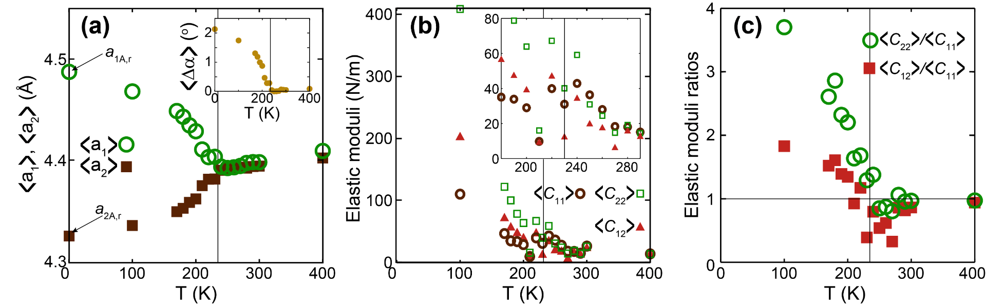
Estimating the elastic behavior of a material across a phase transition
We learn how to calculate elastic constants. But, what is the meaning of an elastic constant across a phase transition? Being more specific, elastic behavior must turn isotropic at a specific phase transition in a 2D material, so elastic moduli have to evolve accordingly. See Publication 63 for a detailed discussion.
Magnetic topological semimetal phase with electronic correlation enhancement in SmSbTe
We verified ARPES results for the electronic structure of SmSbTe, and additional calculations. The material is grown by Colleague Jin Hu. See Publication 62 for more details.
Engineering vortices on ferroelectric/paraelectric SnTe/PbTe lateral heterojunctions
SnTe monolayers grown laterally away from a paraelectric PbTe core end up displaying intrinsic electric fields with a vortex shape. See Publication 61.
A thorough description of ferroelectric group-IV monochalcogenide monolayers in Reviews of Modern Physics
A thorough review on 2D ferroelectrics can be found in Reference 60. (The figure below was created by colleague Kai Chang.)
Discarding ferroelectricity on monochalcogenide monolayers with a (low-buckled) honeycomb lattice structure
Shiva Poudel addressed whether group-IV monochalcogenide monolayers with a honeycomb structure could also be ferroelectric. In short, they are not. See Publication 59.
Exemplifying on a 2D ferroelectric the breakdown of popular DFT-based approaches for thermoelectricity
In the recent past, multiple groups have put in doubt the amazingly large thermal figure of merit (ZT) being reported in calculations based on DFT (see Phase Transformation Contributions to Heat Capacity and Impact on Thermal Diffusivity, Thermal Conductivity, and Thermoelectric Performance. Matthias T. Agne, Peter W. Voorhees, G. Jeffrey Snyder. Advanced Materials 31, 1902980 (2019) for a detailed discussion of the problem).
The main problem is that the most popular (DFT-based) approach for thermoelectricity utilizes zero-temperature vibrational and electronic data and is therefore blind to phase transitions. In experiment, on the other hand, there is mounting evidence that ZT increases precisely at a phase transition! There is a disconnect among most DFT-based modeling and experiment then.
To address this problem, we have generated large amounts of molecular dynamics data; enough to estimate the thermal conductivity across a 2D transformation on SnSe monolayers. In addition, a phase transition also implies that there is a change in the electronic structure.
The figure below, taken from Publication 58, illustrates ZT as obtained with the traditional route; ZT remains anisotropic even at temperatures when the material turned isotropic and it therefore lacks physical meaning. The results with our method peak out near the transition, and then show that the traditional DFT result is actually optimistic. Our methodo could be used to reasses estimations of ZT based on DFT with traditional methods, and may yield results in closer correspondence with experimental observations.
Tuning the critical temperature for the ferroelectric to paraelectric phase transition in 2D ferroelectrics by charge doping
The energy barriers separating two ferroelectric configurations can be increased or decreased at will with appropriate charge doping. This realization has consequences for tuning the critical temperature of those 2D ferroelectrics. See Publication 56.
Creating a special issue on anisotropic 2D materials for the Journal of Applied Physics
Along with Fengnan Xia (Yale), Wenjuan Zhou (Illinois), and Han Wang (Southern Cal), we created a Special Issue on Low-Symmetry and anisotropic materials.
Establishing the theory for phase transitions in 2D ferroelectrics
As it turns out, another model for the phase transition on SnSe monolayers came out after we published our first work on the subject (Publication 38), after our second publication had been posted onto the arXiv (Publication 39), and also after the experimental work by Kai Chang and collaborators. The premise of that work was that the phase transition onto a paraelectric phase takes place in a 2D material that never changes its unit cell but keeps its zero-temperature lattice parameters across a phase transition.
We had established in Publication 43 that the experimental 2D phase transition onto a paraelectric phase requires a coalescence of lattice vectors, but Publication 55 shows the discrepancies among our model (consistent with experiment) and the other one in a definite light: The other model fixes lattice vectors and relies on a single vibration. As such, it is the most constrained model and it yields the largest critical temperature. The experimental situation, nevertheless, requires the lattice vectors to become equal, and it hence is consistent with our predictions only: lattice vectors turn equal at Tc. An intermediate scenario is given by the NVT ensemble (in which the area is fixed, but more vibrations are allowed to contribute to the 2D phase transition).
The phase transition is also shown to depend on the exchange-correlation potentials used in the calculation.
Deploying SnSe monolayers as 2D ferroelectrics
Working with Kai Chang and S. Parkin, we reported the experimental realization of SnSe monolayers on graphene in publication 54. At the point the manuscript published, only other two group-IV ferroelectric monochalcogenide monolayers had been experimentally demonstrated: SnTe monolayers, and SnS monolayers. The figure below illustrates ferroelectric behavior controlled by sudden bias discharges at the STM tip.

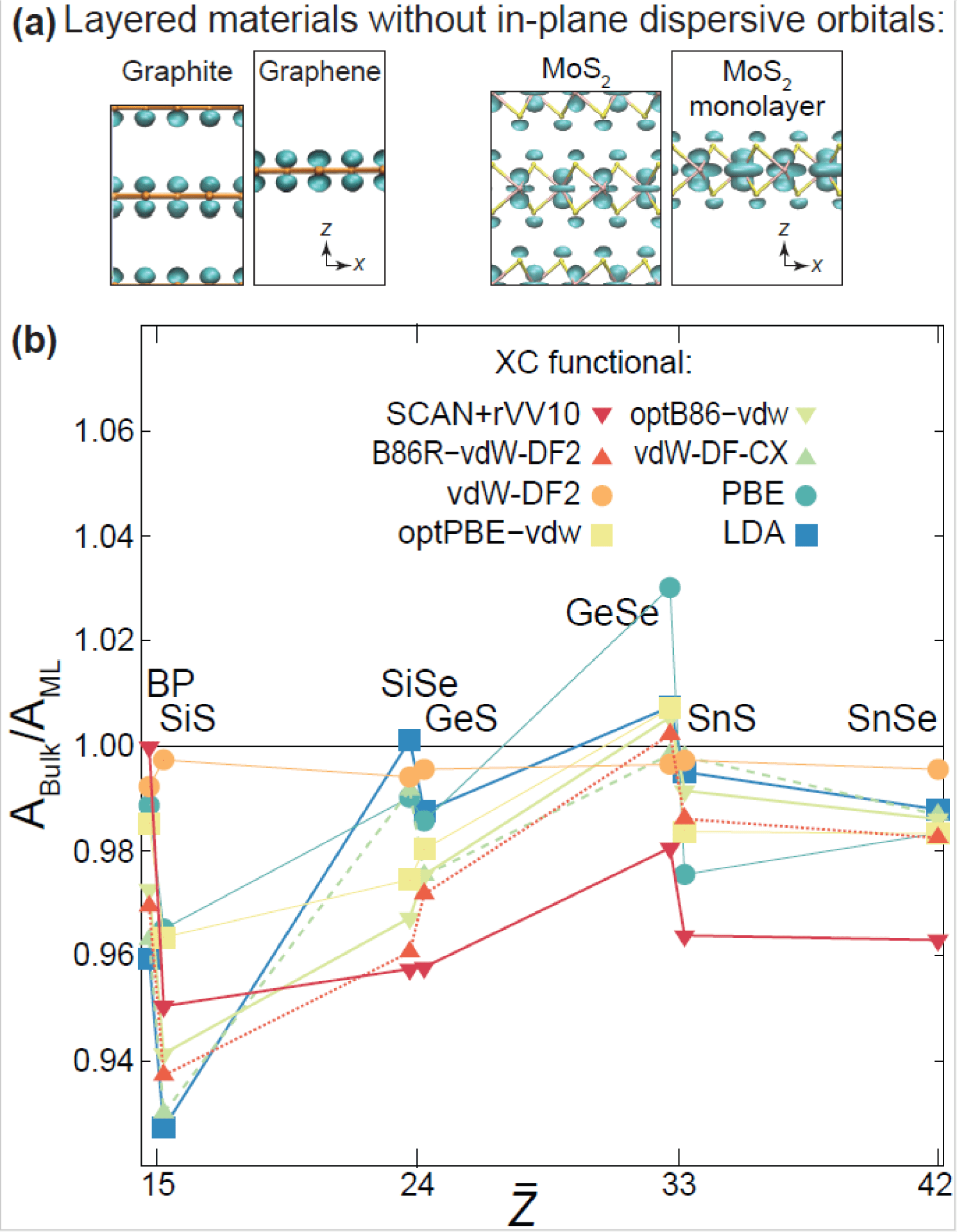
A careful study of the effect of exchange-correlation functionals on the atomistic structure (lattice parameters) of group-IV compounds at the monolayer and bulk limits
Shiva Poudel carried a careful and systematic study of the structure and ferroelectric to paraelectric barriers of multiple monochalcogenide monolayers, using muliple exchange-correlation functionals (see publication 52). He did so because the elastic energy landscape of those materials is rather shallow, and multiple teams reported conflicting values of the lattice parameters even when using the same computational tools.
The figure below shows graphite and graphene, and bulk and monolayer MoS2. Their area does not change when they are thinned down from the bulk down to a single monolayer. Group-IV monochalcogenides, on the other hand, get their unit cell area enlarged as they are thinned down, almost independently of the exchange-correlation functional used (the horizontal axis is the mean atomic number).
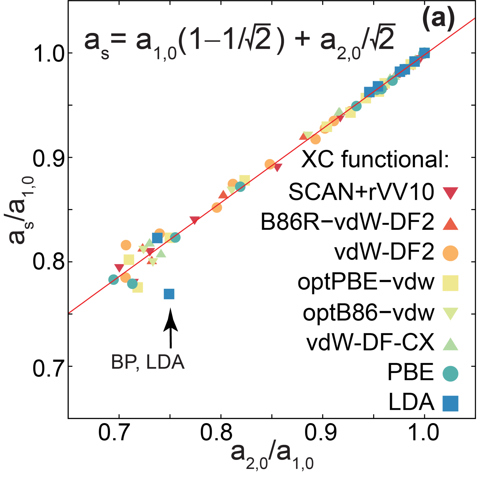
The next figure shows a linear relation among the optimal lattice vectors of the rectangular (ferroelectric) unit cell, and the lattice vectors of the lowes-energy square (paraelectric) unit cell. (The difference in energy among those two structures is used to estimate ferroelectric-to-paraelectric critical temperatures, so knowing the optimal value of the lattice parameter of the square unit cell from those of the rectangular optimal unit cell is important.)
Confining electrons along one spatial direction by mismatched domain walls on ferroelectric SnTe monolayers
I worked with scanning tunneling microscopy (STM) experimentalists during my PhD years, and this work showcases synergistic experimental/theory work with Kai Chang and S. Parkin: The upper figures are STM imgaes of SnTe monolayers grown on graphene on SiC. The image in the middle row of the figure is a supercell of an actual simulated SnTe domain, consistent in size and on the direction of the dipole moment at the domain wall with experiment. The potential energy can be seen as well, and no potential energy buildup can be observed at domain walls.
The structure of the 90-degree domain wall is seen on the lower-left. The figures on the lower right display an interference pattern created at the valence band by the domain walls, from both experiment and our theory.
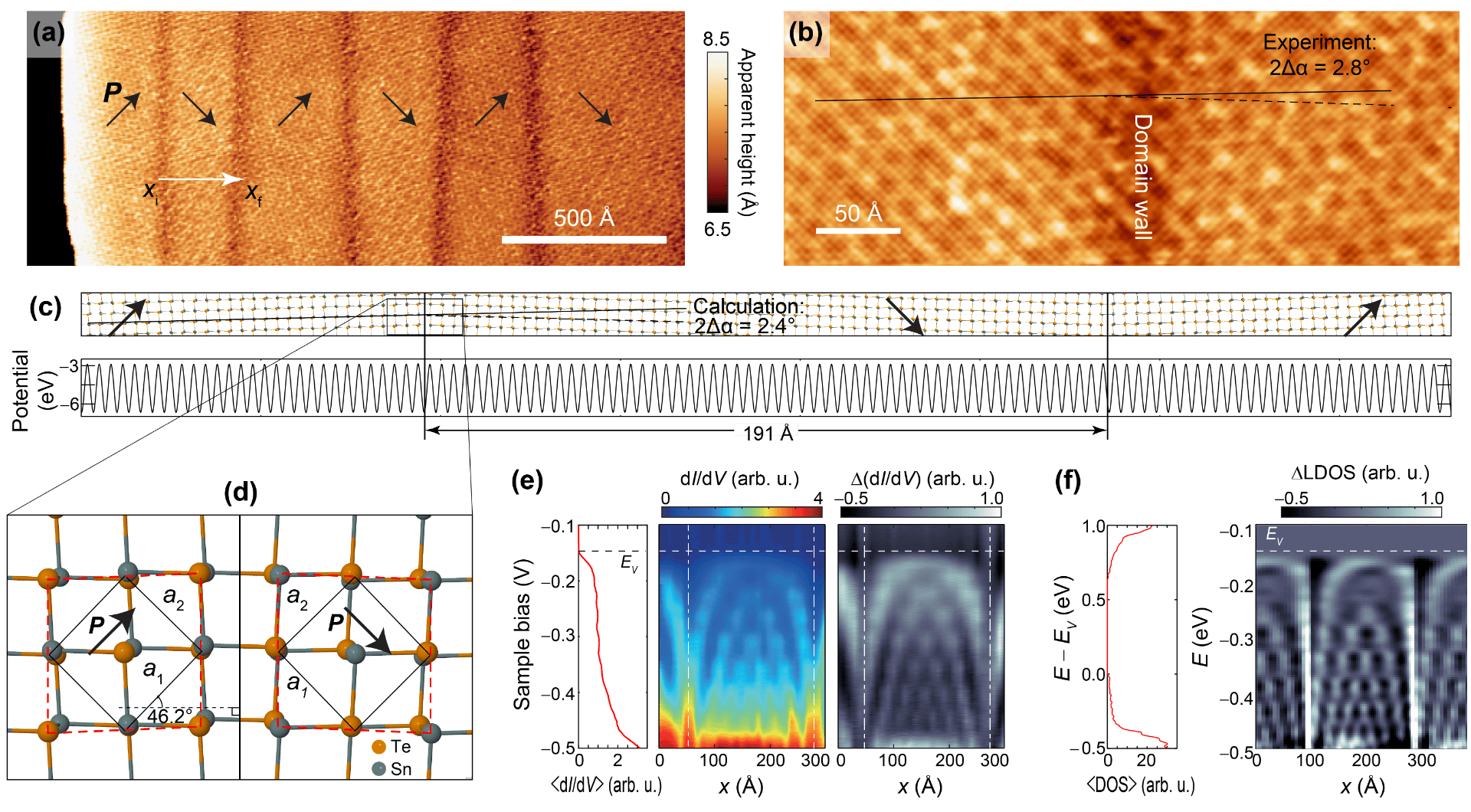
The figure below explains the confinement observed: the valence band has a 0.3 eV energy range where it is dominated by a valley near the X-point. At the domain wall, transmission is not allowed given that the location of the valley rotated by 90 degrees.

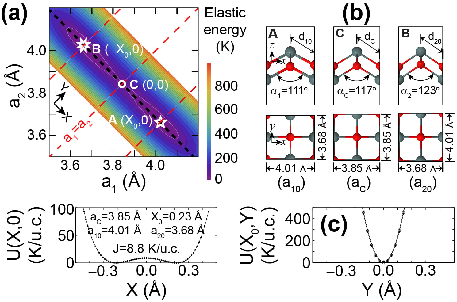
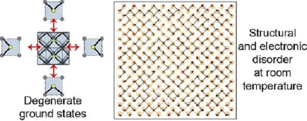
Searching for new phase-changing 2D materials: SnO monolayers are 2D quantum paraelectrics
SnO monolayers were the first materials suggested to be 2D multiferroics by Seixas and collaborators. As seen on the figure below, their unit cell is rectangular and their energy landscape has two degenerate minima. The barrier to switch among those two minima is too small though, so quantum fluctuations preclude the creation of a ferroelastic phase on those 2D materials. See publications 47 and 48.
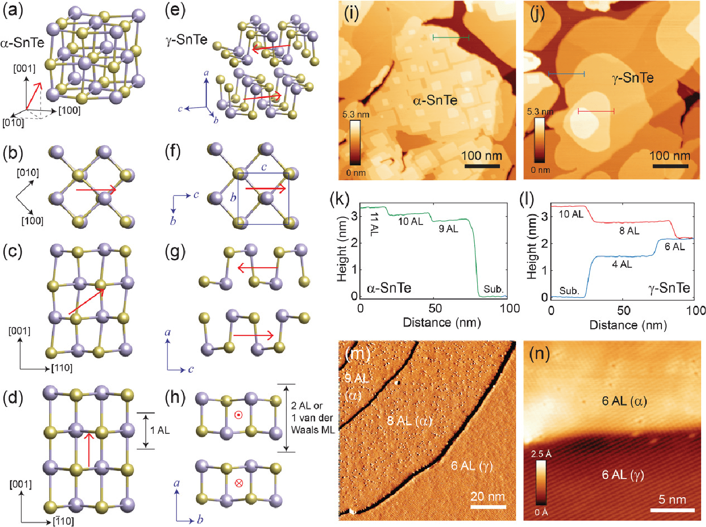
SnTe turns from a rhombic onto an ortorhombic phase as it is thinned down
This work was our first experimental collaboration with Drs. Kai Chang and Stuart Parkin. In publications 46 and 49, we studied a phase change on SnTe. It has a rhombic structure and a dipole along the cube diagonal in the bulk at low temperature but it turns layered and antipolar at ultra-small thicknesses.
Analyzing the propensity toward degradation of group-IV monochalcogenide monolayers
The 2D ferroelectrics isostructural to black phoshorene quickly degrade when in air. We performed ab initio molecular dynamics calculations to understand how polar molecules (water) break as their interact with the built-in electric fields of those 2D ferroelectrics. See Publication 45.
Matching the order parameter of the phase transition in group-IV monochalcogenide monolayers with experimental observation
Our studies of phase transitions in 2D ferroelectric materials allowed for the area of the unit cell to vary at finite temperature. That variation can be captured by the change of a geometrical variable called the rhombic distortion angle Δα. Among other things, we showed in Reference 43 that Δα coalesces to zero at the critical temperature, just like it was experimentally seen in Science 353, 274 (2016). Our theory is the only one consistent with experimental observations.

Verifying the anisotropic electron conductivity of bulk GeSe
The anisotropy of the conduction band valley leads to an anisotropic conductivity on GeSe. This work is part of an experiment-theory collaboration with Wenjuan Zhu’s group at Urbana, and Yia-An’s group at Towson. See publication 42 for more details.
Review on strained graphene and other strained materials
Invited by Gerardo Naumis, I contributed to a Review Article on strained graphene and other strained 2D materials. Below, I highlight the usefulness of the approach based on discrete differential geometry I developed to study graphene under strain.
The upper part on the first figure is taken from: KK Gomes et al. Designer Dirac fermions and topological phases in molecular graphene Nature 483 306 (2012), and it shows a collection of CO molecules on a Cu(111) surface. The CO furnishes a triangular lattice. The graphene lattice is a dual lattice, which is obtained by tesselating the triangular CO lattice.
We noted that in the reference above, the CO lattice was created using a strain profile meant for the honeycomb (dual) lattice.
The lower part on the figure above shows the deviations from a strict displacement leading to a constant pseudomagnetic field when the displacements are applied to the honeycomb and the triangular lattice.
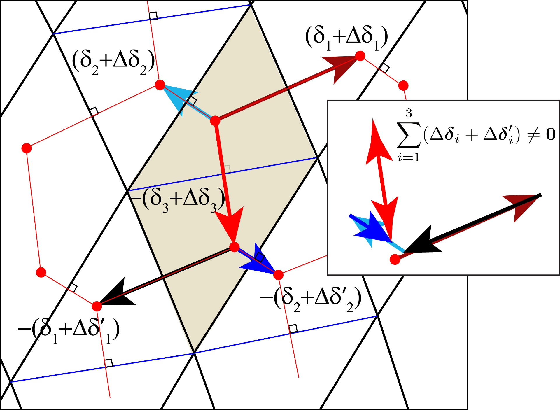
The figure below show phasors not adding up to zero under a very large deformation. This view to strain in graphene can be useful to understand when strain is too large; the usual modeling assumes graphene to be a continuum and it can thus loose connection to the size of the distortion with respect to the atomistic lattice.
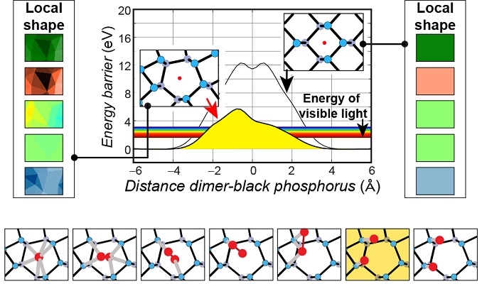
Predicting a significant mechanical effect (photostriction) when illuminating 2D ferroelectric monochalcogenide monolayers
Based on a known effect known in 3D ferroelectrics, we predict a rather large and anisotropic mechanical strain induced by illumination. See publication 40 for details.
Evolution of material properties for few-layer monochalcogenides as a result of a two-dimensional structural transition
Discussing how the properties of few-layer monochalcogenides (ferroelectricity, band structure, and optical properties atomistic structure) evolve as a result of the phase transition we predicted in Reference 38. See publication 39 for more details.
Initial theoretical evidence for phase transitions in 2D ferroelectrics
Any structure with a degenerate structural ground state will display disorder and may undergo phase transitions at a finite temperature. We showed for the first time in 2016, that this is the case for monochalcogenide monolayers; new 2D materials that have a structure similar to a black phosphorus monolayer. See publication 38 for more details.
Linking intrinsic defects to the propensity for photo-oxidation of phosphorene
We found absorption barriers for oxygen molecules to be within the reach of light-induced excitations, and oxygen dissociation at these defects. See publication 35.
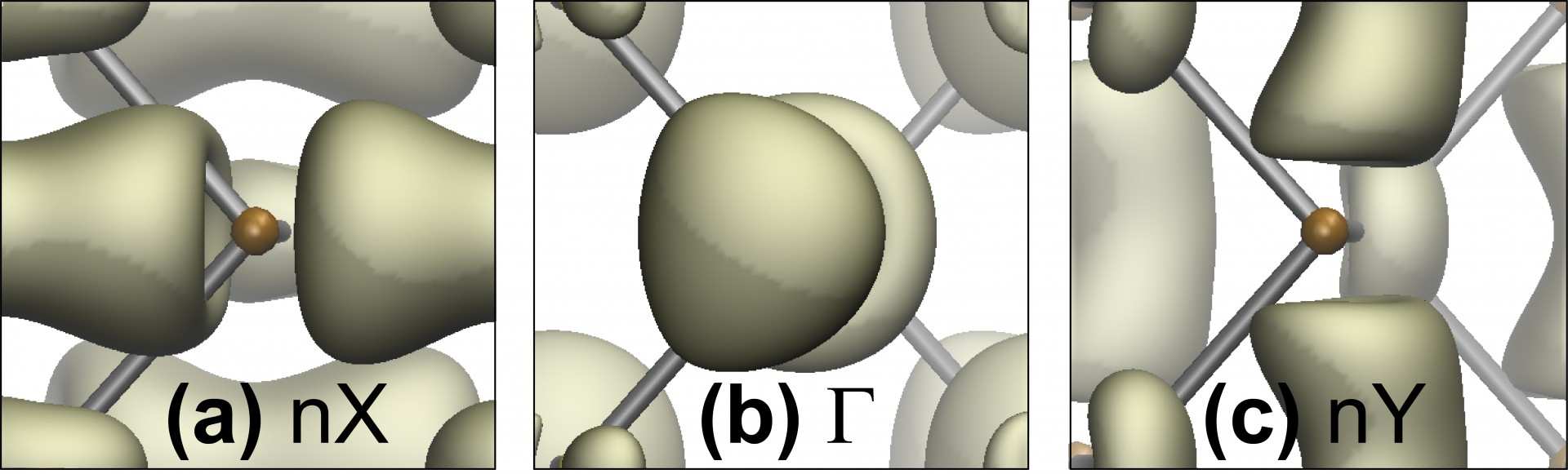
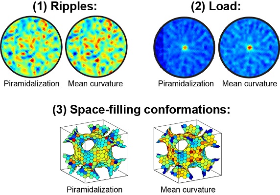
Studying the electronic properties of phosphorene that has intrinsic defects
We created non-planar phosphorene structures by means of intrinsic defects, and characterized the shape and the electronic properties of the material that results from these atomistic defects. See publication 34.
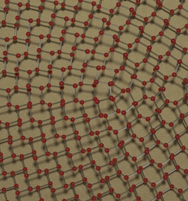
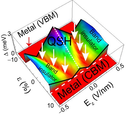
Tuning the electronic gap of silicene by mechanical strain and by external electrostatic fields
There is an electronic coupling among electrons making up sigma-bonds in silicene and the pi-electrons that are responsible for the electronic properties. This coupling leads to an enhancement –and hence tunability– of the spin-orbit coupling of this material as it buckles. See publication 33.
Proposing ways to visualize phosphorene allotropes with a scanning tunneling microscope
Phosphorene is a new two-dimensional material that is highly reactive under ambient conditions. Using a concept we developed back in 2010 (Publication 15), we propose that different two-dimensional allotropes of phosphorene could in principle be told from one another if scanned through a hexagonal boron nitride monolayer that halts the oxidation process. See publication 29.
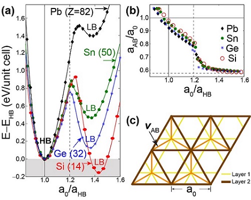
Is stanene stable without a substrate? What is the most stable form of flourinated two-dimensional tin?
We established the structural minima and the properties of stable forms of two-dimensional tin and lead. See publication 28.